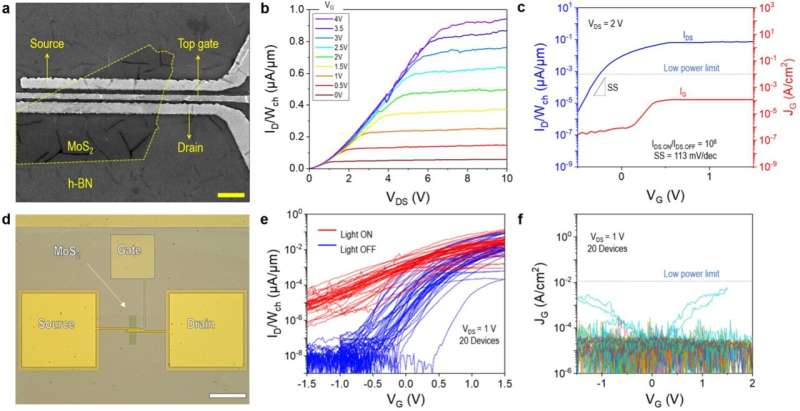
Two-dimensional (2D) semiconducting materials have distinct optoelectronic properties that could be advantageous for the development of ultra-thin and tunable electronic components. Despite their potential advantages over bulk semiconductors, optimally interfacing these materials with gate dielectrics has so far proved challenging, often resulting in interfacial traps that rapidly degrade the performance of transistors.
Researchers at King Abdullah University of Science and Technology (KAUST), Soochow University and other institutes worldwide recently introduced an approach that could enable the fabrication of better performing transistors based on 2D semiconductors. Their proposed design, outlined in a paper in Nature Electronics, entails the use of hexagonal boron nitride (h-BN) dielectrics and metal gate electrodes with a high cohesive energy.
“Initially, we found that when we use platinum (Pt) as an anode, the h-BN stack is less likely to trigger dielectric breakdown,” Yaqing Shen, first author of the paper, told Tech Xplore. “Based on this finding, we designed our experiments and found that Pt/h-BN gate stacks show 500-times lower leakage current than Au/h-BN gate stacks and exhibit a high dielectric strength of at least 25 MV/cm. This gave us the idea of using CVD h-BN as a gate dielectric in 2D transistors.”
Shen, Prof. Mario Lanza and their colleagues fabricated over 1,000 devices using chemical vapor deposited h-BN as dielectrics. When they evaluated these devices, they found that h-BN gate dielectrics were best compatible with high cohesive energy metals, such as Pt and tungsten (W).
“To fabricate transistors with a vertical Pt/h-BN/MoS2 structure, we began by cleaning a SiO2/Si substrate using ultrasonic baths in acetone, alcohol, and deionized water,” explained Shen. “The source and drain electrodes (Ti/Au) were patterned on this substrate using electron beam lithography and deposited by e-beam deposition. Subsequently, MoS2 was exfoliated from a natural crystal and transferred onto these electrodes to form the channel. CVD h-BN film was transferred over this structure through wet transfer.”
As a last step in their transistor fabrication process, the researchers patterned the Pt gate electrode using electron beam lithography and then deposited it using a technique known as e-beam evaporation. The clean van der Waals interface between MoS2 and h-BN in the team’s transistor improves its reliability and performance, minimizing defects and enhancing gate control.
“We discovered that contrary to the belief that CVD h-BN is a poor gate dielectric, selecting the right metal electrodes enables its effective use in field-effect transistors with MoS2 channels,” said Shen. “MoS2 and h-BN form a clean van der Waals interface, which enhances reliability. Our findings show that using high cohesive energy metals like Pt and W makes CVD h-BN an effective gate dielectric in 2D transistors.”
This research team’s approach to fabricating 2D semiconductor-based transistors has so far been found to be highly promising, reducing the leakage of currents and enabling a high dielectric strength of at least 25 MV cm-1. Initial tests revealed that Pt and W-based gate electrodes reduced the leakage current across h-BN dielectrics by a factor of approximately 500 compared to similar transistors with gold (Au) electrodes.
The recent work by Shen and her colleagues could facilitate the use of 2D materials for fabricating reliable solid-state microelectronic circuits and devices. Other research groups could soon explore similar approaches and materials, which may lead to the development of further highly performing 2D semiconductor-based devices.
“As the next step in our research, we plan to develop ultra-small (nanoscale), fully 2D transistors to help extend Moore’s Law,” added Shen. “We also aim to solve the contact issues between 2D channels and electrodes to enhance device performance.”
More information:
Yaqing Shen et al, Two-dimensional-materials-based transistors using hexagonal boron nitride dielectrics and metal gate electrodes with high cohesive energy. Nature Electronics(2024). DOI: 10.1038/s41928-024-01233-w
© 2024 Science X Network
Researchers develop approach to fabricate highly performing transistors based on 2D semiconductors (2024, September 7)
retrieved 7 September 2024
from https://techxplore.com/news/2024-09-approach-fabricate-highly-transistors-based.html
part may be reproduced without the written permission. The content is provided for information purposes only.


